Our experts: Jaime Diez Merida (LMU), Dmitri Efetov (LMU), Maelle Kapfer (UPSaclay), Gaia Maffione (UPSaclay) and Rebeca Ribeiro-Palau (CNRS)
Clean exfoliated 2D materials are the first step to a great van der Waals heterostructure. There are many tricks to it but the real way to do a great exfoliation is experience! Of course the right type of tape and a clean substrate also help.

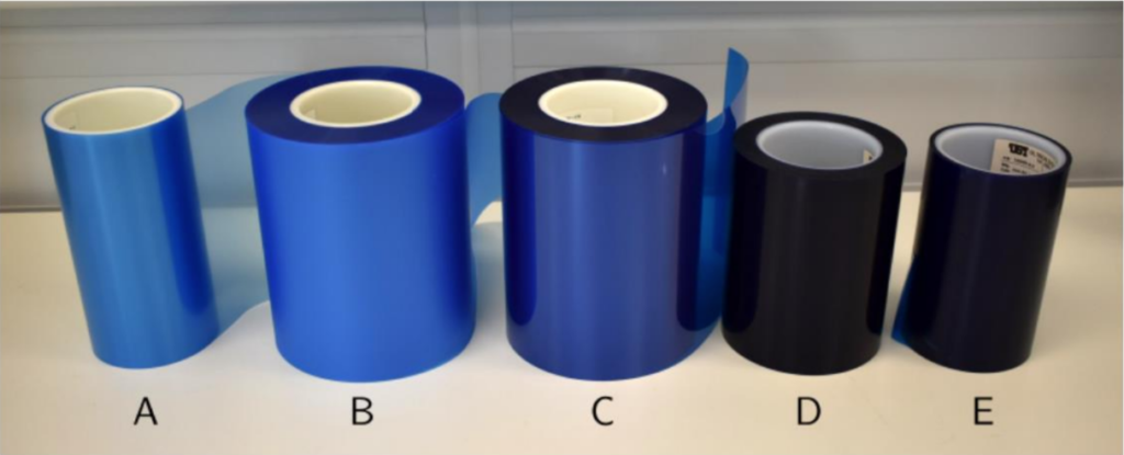
Choose your tape: This is a long lasting controversy since many research groups use blue clean room tape and others regular scotch tape. There is not major difference between these two since most of the research groups are able to obtain clean flakes but here once again you should make your own experience and try different tapes since the results can vary depending on the humidity and temperature of the room where you are exfoliating.
Heating technique: in order to obtain large area monolayer and bilayer graphene and other 2D materials it is highly recommended to use the technique developed in this article. In short, you will need to clean your Si/SiO2 chips in a soft oxygen plasma before approaching the tape with your exfoliated material, once in contact you will need to heat them up in a hot plate at ~100 oC for about 2 minutes, let them cool down after and pill off the tape.
BN exfoliation: for BN exfolaition (not too thin flakes) the process is the same but without heating the substrate before pilling off the tape. Avoiding heating leave cleaner flakes in the case of BN.
Pro-tips:
- Make sure, if you are using a RIE, that the plasma is not too strong and don’t do it for long, we normally use 20-30 s, otherwise the pickup becomes very difficult.
- Press gently with your tumb the tape while the chips are in the hot plate to get a better contact of the exfoliated material with the tape.
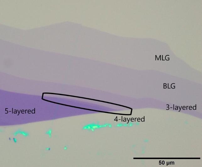
Identifying the number of layers: Following the exfoliation process, the number of layers on a flake can be identified using their optical contrast with the substrate when observing with an optical microscope. The amplitude of the contrast will depend on the material (graphene, BN…), the substrate (for example thickness of SiO2) and the wavelength of the illuminating light [reference article]. When high enough, the contrast will present discrete steps whose amplitude is directly linked to the number of layers.
Pro tips:
You quantify the contrast of a monolayer of your material by using a software like ImageJ. For this split the channels by color (Red, Blue, Green) and trace a line covering different thicknesses and extract the monolayer thickness.

Additionally, Atomic Force Microscopy (AFM) topography can be combined with the optical contrast to determine the number of layers on a flake. This is especially helpful when characterizing a new material whose contrast with the substrate is unknown.
Finally, Raman spectroscopy can be particularly useful to identify monolayers [reference article].
While contrast is a powerful and most notably fast way of identifying layer number, it tends to saturate for high number of layers where AFM topography will give the exact thickness of the flake.
Lastly in some cases, given any combination of substrate and light wavelength, the optical contrast can remain low, this is for example the case of monolayer BN, and other methods are necessary to identify monolayers.
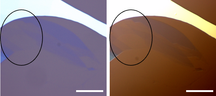
Particularly hard to find, monolayer BN: monolayer and thin BN are specially difficult to obtain and to find with an optical microscope. In our experience (and already documented in the literature here), the best way to obtain monolayer graphene is by using the heating technique explained before. Doing this in a 90 nm SiO2 layer will allow you to have enough contrast to see the monolayers, to improve their visibility you can use a U-DICR polarizer.
Stacking of 2D materials:
Before starting to stack your 2D materials you should think in what type of stack you want to do and what are the more appropriated methods to do so. Here are some examples:
Stacking to a fragile substrate (e.g., TEM grid): For this you migth want to use the membrane transfer. This one consist in exfoliating in a polymer and releasing this as a membrane to later deposit it the target substrate. You can find all the details in this article and its supplementary.
Stamping: This is the so called dry technique and consists in using a 2D material to pick up sucesive 2D materials. One of the first publications to explain the technique is here. The animation below is very self-explanatory of the process.
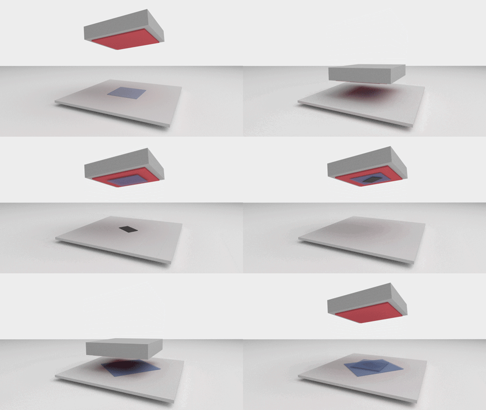
The process consist in picking up the different 2D materials one at the time using a combination of polymers (e.g., PPC or PC on top of PDMS). After picking up all the different 2D materials the polymer is melted on top and the stack deposited on the substrate of your preference.
The hot pick up technique (under construction):
Bubble squeezing: After picking up all the layers you might realize that some bubbles are formed in your stack. This are formed of tape residues, water and/or air. To clean up your stack you can squeeze the bubbles mechanically at higher temperatures. The techniques to do this (either with PC or PPC) are described in the following article. As you can see in the pictures bellow the technique is very effective to get ride of bubbles
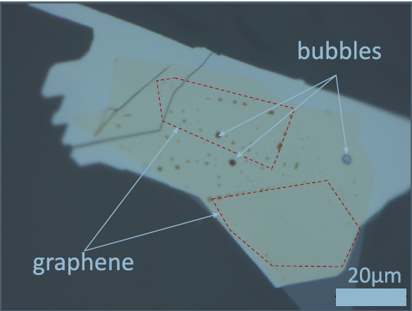
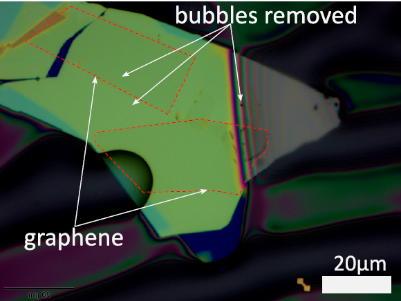
PDMS stamping: As you could see all along this post we have mentioned two main polymers PC and PPC that are deposited on top of PDMS, these are the most used ones in for the stacking. However, there are other polymers also used for this, in the following table we summarize them and give you their main use and temeprature range to be used.
| Polymer | Temperature pick-up | Temperature release | Cleaning |
| PPC Ploy(propylene carbonate) | 40 oC | 80 oC – 120 oC | Annealing in vacuum at 360 oC |
| PC Polycarbonate | 80 oC | 180 oC | Chloroform |
| PET Poly(ethylene terephthalate) | 60 oC | 130 oC | |
| PVC Poly(vinyl choride) | 70 oC | 130 oC | |
| PCL Poly(caproalactone) | 30 oC | 60 oC |
TWISTING!
Now that you have the basic notions of stacking you can start preparing twisting heterostructures. For twisted graphene structures the most widely used technique is the tear and stack technique detailed here. However, the tear part of this technique has been proven to give many problems of breakign the layers. A clear improvement in reproducibility has come with the implementation of different techniques to cut graphene before starting the stacking. Here we list few of them:
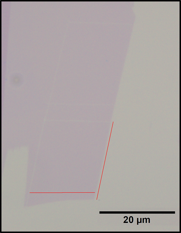
- AFM cutting: the anodic oxidation nanolithography consist in applying a high frequency (>10 kHz) AC voltage to a Pt/Ir coated AFM tip (e.g., Arrow-NCPt-50, available here), to design on it a desired pattern, the resolution of the cut can go down to 10 nm, which makes it particularly interesting for polymer-free lithography of graphene. The full explaination can be found in this research article. An example of what can be done in graphene:
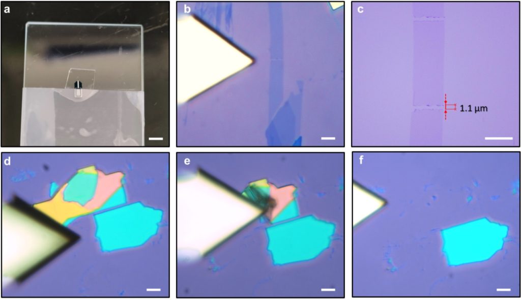
- AFM tip on PDMS cutting: A cheaper version of this technique can be achieved by sticking an AFM tip to a PDMS stamp. The PDMS stamp is placed in a transfer station, the optical microscope of this allows you to see when the tip enters in contact by a change in its reflectance. Once in contact the stage is moved to cut the graphene or move pieces of 2D materials that you don’t want in the way, as depicted in the picture below.
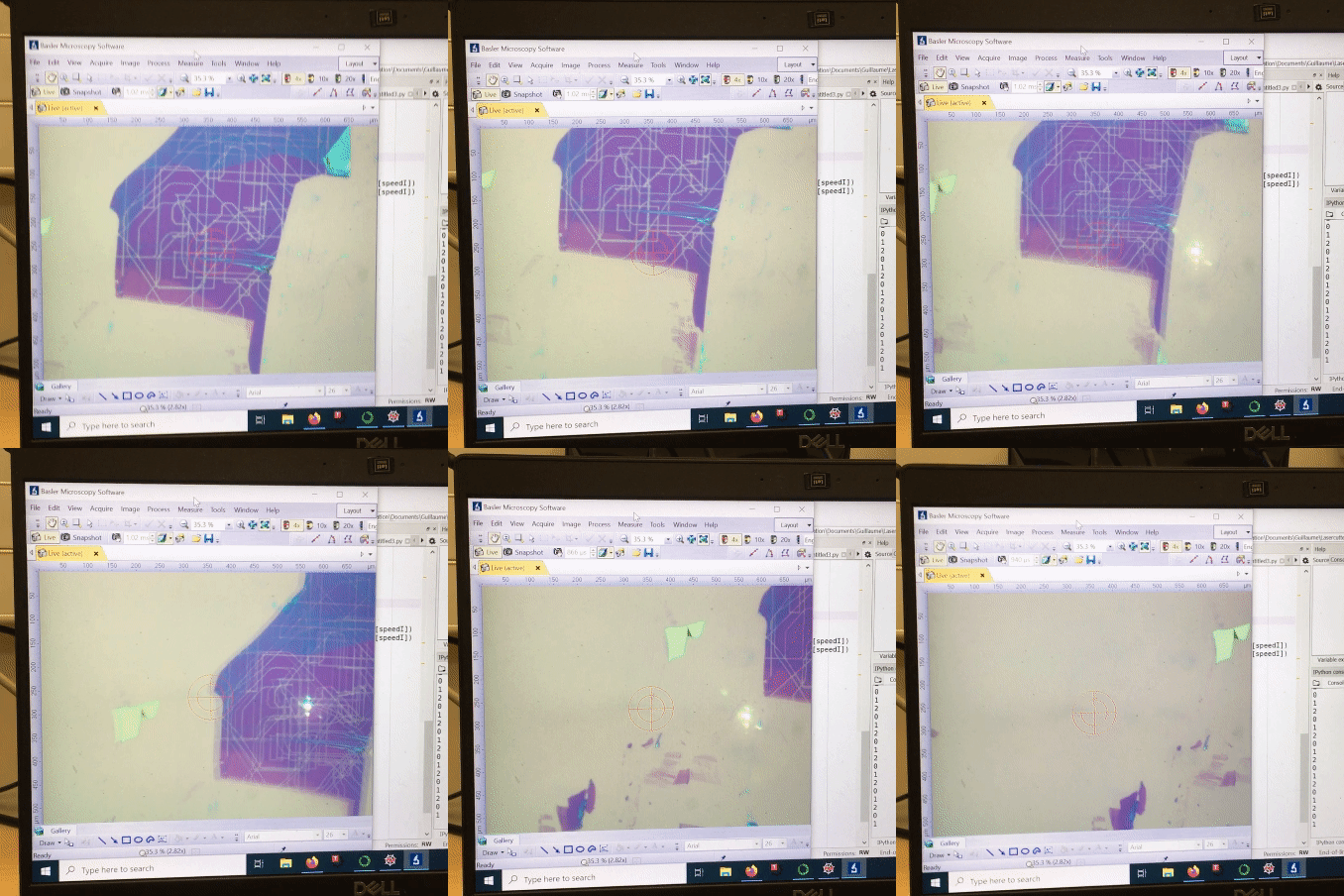
- Laser cutting: by using a laser (filters between 500 nm and 600 nm) we can perform cuts in graphene and graphite layers in a fast and easy way. This technique was developed by Lutz Waldecker at RWTH and we added a joystick to to make it easier to use:
Rotatable structures
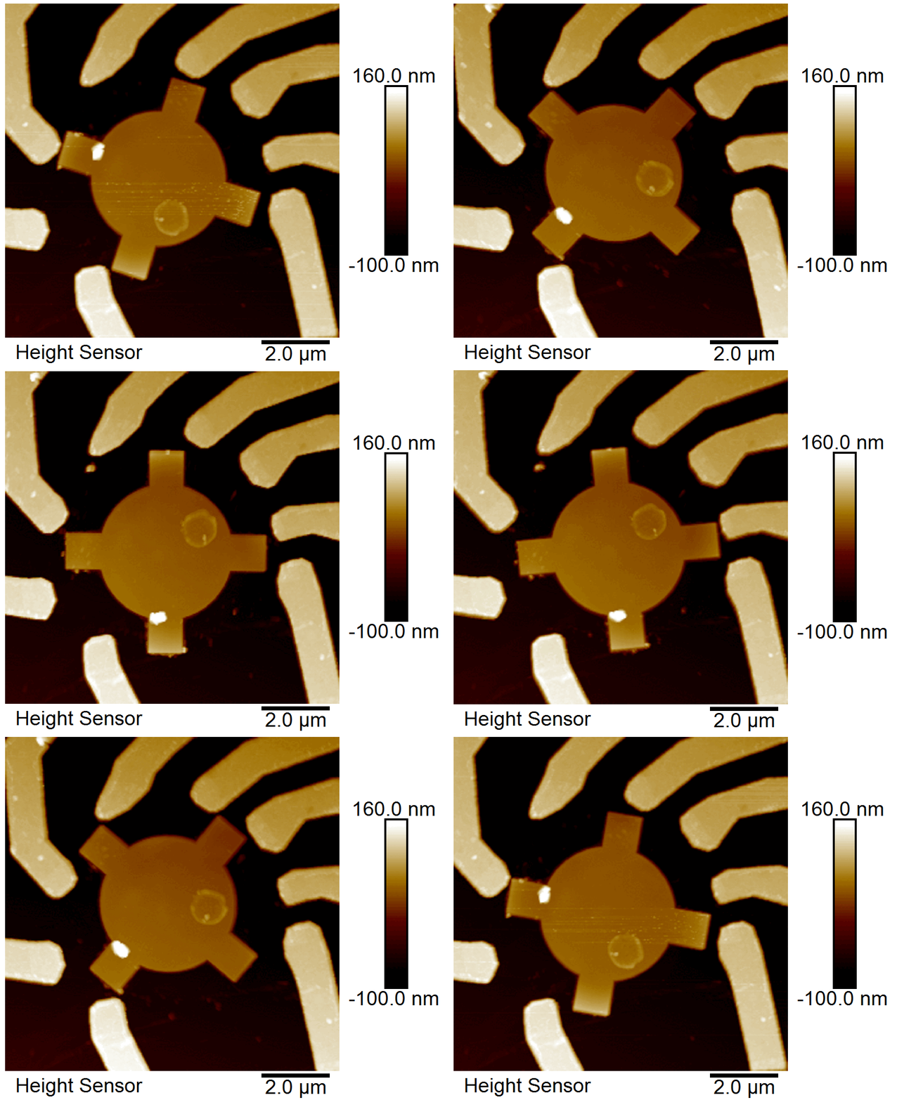
The techniaues presented before are useful to build static angle van der Waals heterostructures, however, it is possible to control the angle dynamically. This will allow to investigate the evolution of the properties if a heterostructure as a function of the twist angle. Although the twisted bilayer version of this technique is still under development by our consortium, in this article you can find the decription of the technique applied to graphene/BN twisted structures.

Imaging moire superlattices
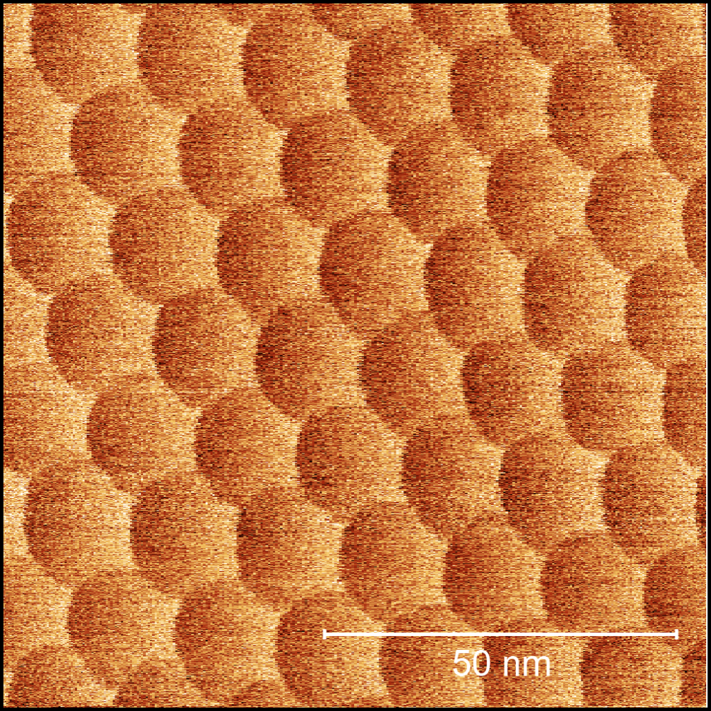
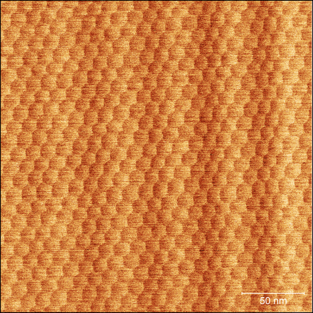
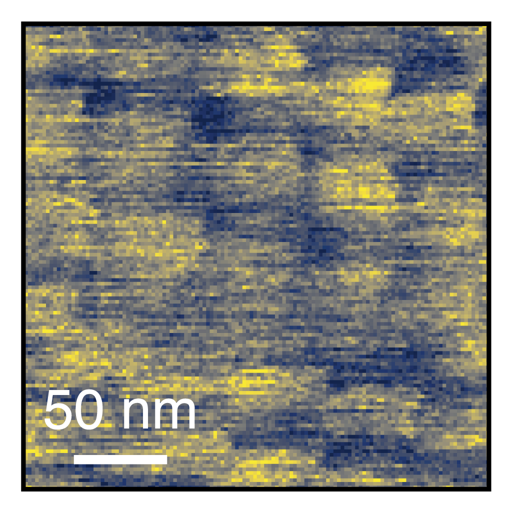
When fabricating twisted heterostructures it is essential to be able to characterize the twist angle throughout the stacking process. Currently AFM imaging techniques are being used. While some techniques offer high contrast between moiré domains for a wide range of materials and twist angles such as conducting AFM (reference and ArXiv) and Scanning Microwave Impedance Microscopy (reference) those either require an electrical contact to the heterostructure or specialized equipment.
Contact mode imaging is then the ideal way to image moiré as no electrical contact is required and can be done either on when the stack is on a SiO2 chip (left picture) or directly on the PDMS stamp used for stacking (right picture). Techniques such as Piezo-Force Microscopy [reference], Lateral Force Microscopy (LFM) and Torsional Force Microscopy (TFM) [reference] will give high contrast between moiré domains depending on the tip used (soft for LFM for example) and the normal force applied on the twisted structure (high for TFM).
