Our Experts: Antonella Cavanna (CNRS), Nicolas Reckinger (UCLouvain) and Zhenxing Wang (AMO)
In order to move graphene technologies from the experimental labs to the real technological world we will need to start producing our devices in larger surfaces with a high reproducibility. In order to achieve the large surfaces one of the most used methods is the chemical vapor deposition, or CVD, growth. In the following we will describe the main ingredients for the growth and the advances we have made to improve its quality and to transfer it from its native substrate to any other.
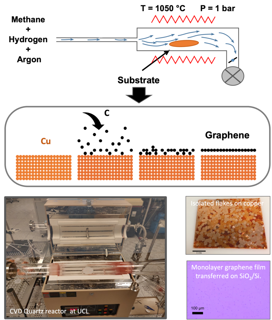
Graphene grown by chemical vapor deposition – Principle of growth:
Quartz reactor pumped to primary vacuum and returned to atmospheric pressure with argon. Copper foil as catalyst. The furnace is heated to 1050°C. Once 1050°C has been reached in the tube, methane and hydrogen are introduced in addition to argon. After a growth time of one to several hours, the tube is slowly cooled down to room temperature.

Improving the quality of CVD graphene on Cu
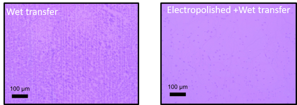
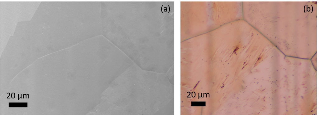
We have conducted a thorough study on the origin of the unavoidable contaminations at the surface of copper after the CVD process. We have identified two distinct origins for the impurities. The first type is intrinsic impurities, originating from the manufacturing process of the copper foils, already present at the surface before any high-temperature treatment, or buried into the bulk of copper foils. The buried impurities diffuse towards the copper surface during high-temperature treatment and precipitate. The second source is external: silica contamination arising from the quartz tube that also precipitates on copper. The problem of the extrinsic silica contamination is readily solved upon using adequate confinement of the copper foil samples. The intrinsic impurities are much more difficult to remove since they appear spread in the whole foil. Nevertheless, electropolishing proves particularly efficient in drastically reducing the issue (see figure below for comparison). The results of this study are published in N. Reckinger and B. Hackens, Appl. Surf. Sci. 641, 158555 (2023).

Graphene exfoliation from copper and transfer to another substrate
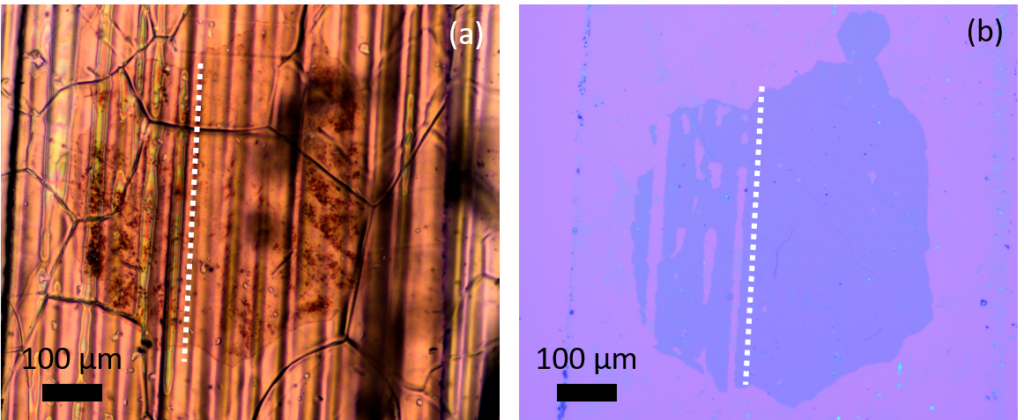
A polymer-based stamp on a glass slide fixed to a home-made micromanipulator is used to perform dry exfoliation of isolated single-layer graphene flakes (several hundreds of microns in size) grown on copper by chemical vapor deposition. The graphene/copper substrate is immersed beforehand in an aqueous mixture for several hours to oxidize the copper layer underlying graphene.

After exfoliation, the graphene flake is transfered onto a 300-nm-thick SiO2/Si substrate. One can see that graphene on deeper copper grooves (rolling striations) stays on copper because the polymer is not in contact with graphene before exfoliation. Even though the copper foil is electropolished, the striations still persist. Nevertheless, a sizable chunk of graphene could be exfoliated and nicely transfered.

