Our Experts: Sofiane Arib (UCLouvain), Maelle Kapfer (UPSaclay), Gaia Maffione (UPSaclay) and Rebeca Ribeiro-Palau (CNRS)
All you need to know to prepare a good device for electronic transport. The first important thing is for you to know what is this device for and what are the characteristics you want, but keep it realistic. Since the fabrication process will mainly depend on the tools you have at hand in your clean room here we will mention the main problems we have encountered over the years.
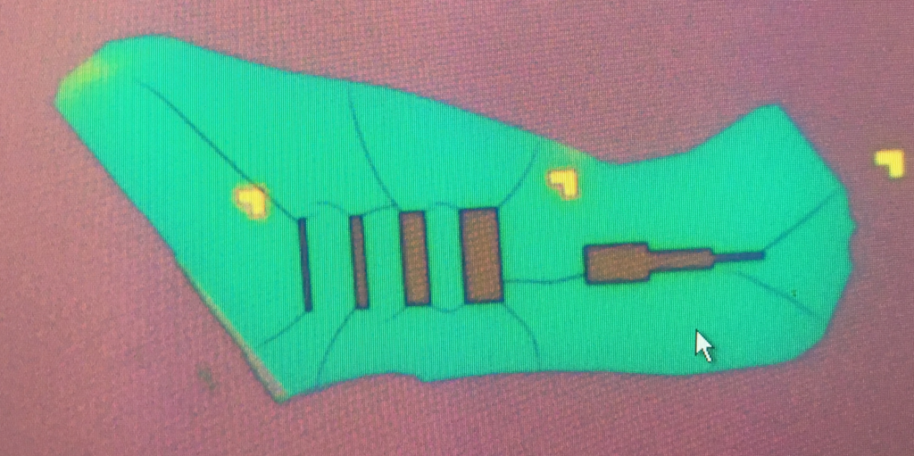
BN cracks: One common problem we faced a while ago was the cracks on the BN after e-beam lithography. Here we show you a extreme example of it where the cracks in the resist were deep enough to create trenches during the etching process.

There is one way to reduce this is by avoiding hard angles in your lithography. This simply mean that instead you should make round corners, this will strongly reduce the number of cracks in the resist. However, there is another way that will eliminate this problem: using IPA:H2O developper. This developper generates less strain than most common developpers (e.g., MIBK:IPA). Some references about this are here.
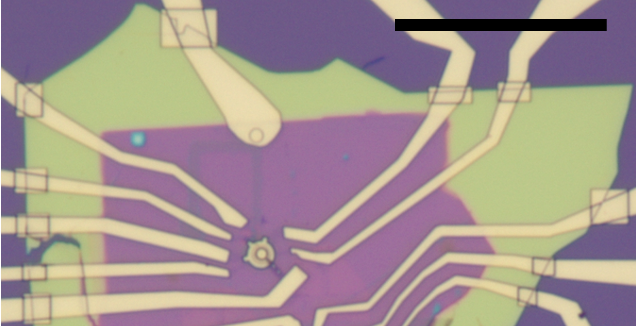
Hard edges of BN will break your electrical contacts: The hard edges of BN, specially if it is too tick, could break your contacts and you will need to repeatedly add patches, as in the picture. To avoid this a simple etching around the edges of the device will create the 45 degrees profile and create a smooth step for your contacts to climb.

SF6 versus CHF3 etching advantages and disavantages: Shaping the heterostructure into a Hall bar for electrical transport measurements is usually done using Reactive Ion Etching (RIE). Plasma formed from CHF3 or SF6 can be used to etch the encapsulating hBN and expose the graphene. The different chemistry will result in different etching rate and etch angle.
However, the main difference is that SF6 does not etch graphene while CHF3 does. This means that shaping graphene heterostructures with CHF3 will results in the usual edge contact while SF6 will result in so-called “mezzanine” contacts where only the top hBN is etched and the graphene is etched by a short O2 plasma step.Etching with SF6 is fast with etch rate of the order of ~ 100s of nm/mn but cracks in the graphene can lead to over etching and shorting the channel to the bottom graphite gate if used. Because of the small etch rate using CHF3, ~ 10s nm/mn, shorts to the back gate are less likely to happen.
Metal gates versus graphite gates: it is now well stablished that metal gates induce a certain amount of disorder given their inhomogeneous profile. This effects have been seeing in the fractional Hall effect in monolayer graphene (here). More recently this has also being tested in bilayer graphene (here).
Advices on etching physical constrictions: The constrictions are physically created by etching the sample and have a typical width around 300 nm. This step requires particular care due to the risk of completely closing the constriction and rendering the sample unusable. The only way to avoid this is by testing your lithography and etching parameters directly in a BN layer. Having a well calibrated BN etch rate is also very important. Here is an example of the physical constrictions created by the consortium in twisted bilayer graphene.

Breaking the SiO2 during wire bonding: a critical (and very frustrating) step before measuring our devices is to wire bond it to a sample holder. The most common problem is to break the SiO2, the causes of this are many e.g., the force and/or ultrasound power are too high, the needle is broken, etc. In order to avoid this problems you should test the bonding machine first in empty connection pads – we strongly recommend you to leave some pads that are not connected to your sample. Once you have the good parameters there is one last critical parameter that we recommend you to look at before you do the bonding, the humidity of the room. In our experience keeping the humidity of the room above 50 % RH while bonding improved the yield of bonding and decreses the risk of breaking the SiO2.
Geometrical advices coming from metrological devices. (under development)
